
Interesting marketing that works
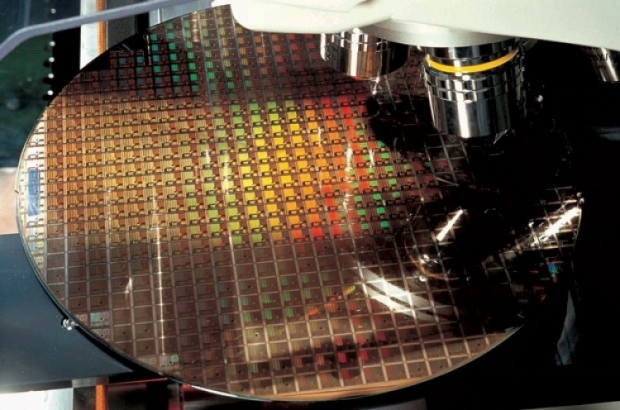
I have been around to vividly remember 350 nm and the first Pentium and AMD K5/K6 processors, and since that time, I have tracked the microprocessors and GPU market. It went swiftly from 350 to 250nm and later to 180, 130, 90, 65, 45, 32nm, and 14nm. It took some ten significant geometry shrinking and power reductions to get to 10nm and even to get to 7nm. Apple, in collaboration with TSMC, is just months away from announcing 5nm chips, but the real question is, do nanometers matter?
We have all been fixated on smaller numbers. It plays well in your mind that 7nm is better than 10nm or 14nm, but the reality could not be further from that logic.
A smaller geometry, let’s take 7nm as an example, means more transistors per square millimeter, higher density, potentially higher clock, and TDP and lower transistor voltage. This is all in theory as there are so many factors that play an essential role
TSMC vs Intel nomenclature
Let’s address the elephant in the room. What TSMC calls 10 nm corresponds to what Intel calls 14nm. What TSMC and its partners call 7nm is close to 10nm at Intel.
The Nvidia Turing is TSMC 12nm, and since the chip launched more than eighteen months ago, if nanometers were the only metric, it should not win against big Vega Radeon VII cards. Of course, this was not the case as Nvidia managed to make a better IPC ratio despite the disadvantage of the transistor size, voltage, and density. Architecture plays a key role in the success of the chip. Nvidia managed to get the better end in 12nm versus AMD’s highest power Navi chip in 7nm. Jonah Alben is hard to beat.
The Nvidia Ampere is now 7nm, and once Nvidia announces consumer GPUs, it will be interesting how it will compare with AMD’s next-generation big Navi GPU, manufactured in 7nm. In this case, both companies will be at the same manufacturing geometry, but one will end up being faster.
It will all be down to the architectural decisions and tradeoffs, which makes better gates and chip blocks to run the workload faster at the given transistor count and overall power.
5 nm at TSMC is Intel’s 7nm
Apple is expected to announce 5nm A13 in September 2020, while Qualcomm Snapdragon 875 is expected to use the same geometry and launch later this year, most likely December. Huawei might be left out of 5nm chips due to the embargoes, but usually, the company is among the first wave customers to go for the smallest transistor.
There is a pattern here. Apple goes toward the smallest geometry since mobile phone designs are very power constrained, and in an iPhone, you have a 2W TDP for the chip. Compare that to a notebook that might still get passively cooling with 7 to 9W TDP. A 2W TDP is not a lot, and this is one of the key reasons why Apple, Qualcomm, and Huawei, when allowed, are the first to go after the smallest transistor.
Smaller geometry can increase battery life as the transistor gets higher power, and geometrically, one can place more transistors on the same surface.
ATI/AMD and Nvidia used to be the first to go after the smallest transistors as they have a power TDP limitation. GPUs can use as much power as you can throw their way, as there will always be a need for higher resolution, higher framerate. Bear in mind that 4K 3840×2160 resolution at 60Hz is four times Full HD 1920×1080 60 Hz. There are four times more things to calculate, and 8K – once we get there – will be four times 4K or 16X more computationally demanding than Full HD.
One of the reasons why GPUs have been used in AI and Machine learning workloads is the fact that they are designed to process vast amounts of data, have fast internal interconnect, fast memory, and a lot of bandwidth.
The CPU and the transistor myth
AMD Ryzen 3000 series codenamed Matisse has been prominent and known for its 7nm TSMC manufacturing even though the I/O part of the chip is manufactured in 12nm. A significant part of the chiplet approach is not 7nm, and yet, everyone calls the CPU 7nm. I/O controller includes dual-channel DDR4 memory controller, PCI-Express gen 4.0, integrated southbridge too. The southbridge part alone takes care of two SATA 6 Gbps ports, four USB 3.1 Gen 2 ports, LPCIO (ISA), and SPI (for the UEFI BIOS ROM chip).
The second-generation Ryzen 3000 called Ryzen 3000 XT will ship in some two weeks, and uses the same 7nm. AMD confirmed that Zen 3 codenamed Vermeer (Ryzen 4000) will launch in 2020, so later this year.
Intel’s latest desktop chip Comet Lake – S is 14nm and just looking at the manufacturing marketing number. Bearing in mind that Intel’s 14nm corresponds mostly to what TSMC calls 10nm, this would give Ryzen 3000 Matisse processors an edge, but yet Matisse loses in gaming and in most single treaded workloads where instruction per clock matters. AMD wins in workloads such as rendering where more cores count. Ryzen 9 3950X has sixteen cores and in rendering defeated Core i9 10900K (10 core) solution.
Marketing plays a vital role here as there is a percentage of people who actually use rendering, but in marketing, it is all about who gets the highest Cinebench score. For end users answering emails, writing documents, and watching pictures and Netflix, sixteen cores won’t help much. Ironically more cores won’t help in gaming either, one very demanding use case. Bright architecture and single-threaded IPC will.
AMD’s XT processors might improve single treaded and gaming performance over Intel’s Comet Lake-S, but Intel is expected to follow with the Rocket Lake-S powered with the new architecture. The first rumors about asynchronous big and small core approach with Alder Lake sound very innovative and exciting in the X86 arena.
Mobile laptop market
Intel is at 10nm first with Ice Lake, now with extreme power saving Lakefield and soon with the second-generation 10nm+ Tiger Lake.
AMD is at 7nm with its mobile offering, and in 2020 it announced a range of Ryzen 3 to 9 laptop solutions covering 10 to 54W TPD market. The 7 nm Renoir microarchitecture is a huge step forward for AMD, but it still fails to discredit and outperform Ice Lake in most workloads that matter.
AMD will continue improving, but first indications of 10nm+ Tiger Lake and the fact you can game well at 1080P in AAA titles such as Battlefield V will put additional pressure on AMD’s notebook efforts. Tiger Lake already has more than 50 design wins.
Most importantly, it is using the new Willow Cove CPU cores, one that will be better optimized for AI and today’s workload.
So 10nm from Intel in laptops bests 7nm AMD solution, proving the general thesis that 7nm is TSMC’s number and looks good.
It is somewhat embarrassing that 7nm second-generation Ryzen cannot beat Comet Lake – S, a 14nm massively improved but with general Skylake DNA, more than five years old. Intel found a way to optimize the transistors, workloads, and clock above 5GHz, something that was enough to help them win in most games and single-threaded apps.
The competition is fantastic, and having AMD breathing down Intel’s neck is excellent for the industry. It looks like Intel gradually is going to smaller nodes when it makes sense. It started in mobile/laptop computers, and now it is about to do the same for the server market where power and density play a significant role. The desktop might follow in the next year with its first 10nm.
It will be interesting to see if the rumors that Intel’s Rocket Lake-S gets the new architecture and still sway at 14nm implies an important change at Intel. The core designed initially for 10nm might find its way to 14nm. It is questionable is that core derived from Sunny or Willow Cove, but we will know this soon enough. It will be interesting to see the new core architecture fighting Zen 3 Vermeer later this year.
The general conclusion is those chip makers should focus on performance and not manufacturing nanometer marketing. It is all about performance for the given workload.


